- English
- Español
- Português
- русский
- Français
- 日本語
- Deutsch
- tiếng Việt
- Italiano
- Nederlands
- ภาษาไทย
- Polski
- 한국어
- Svenska
- magyar
- Malay
- বাংলা ভাষার
- Dansk
- Suomi
- हिन्दी
- Pilipino
- Türkçe
- Gaeilge
- العربية
- Indonesia
- Norsk
- تمل
- český
- ελληνικά
- український
- Javanese
- فارسی
- தமிழ்
- తెలుగు
- नेपाली
- Burmese
- български
- ລາວ
- Latine
- Қазақша
- Euskal
- Azərbaycan
- Slovenský jazyk
- Македонски
- Lietuvos
- Eesti Keel
- Română
- Slovenski
- मराठी
- Srpski језик

China Desain dan tata letak PCB produsen, pemasok, pabrik
Hitech as one of the professional China PCB Design and Layout manufacturers and China PCB Design and Layout factory, we are strong strength and complete management.
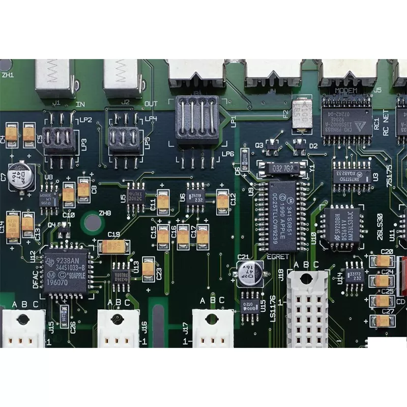
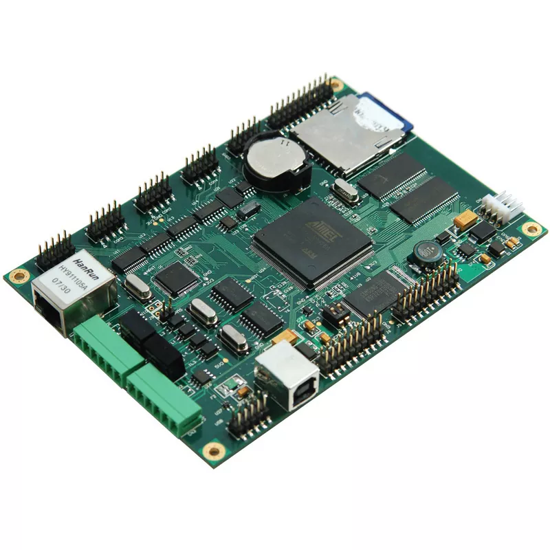
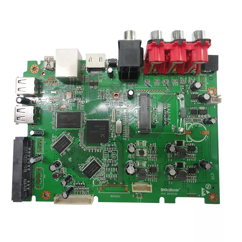
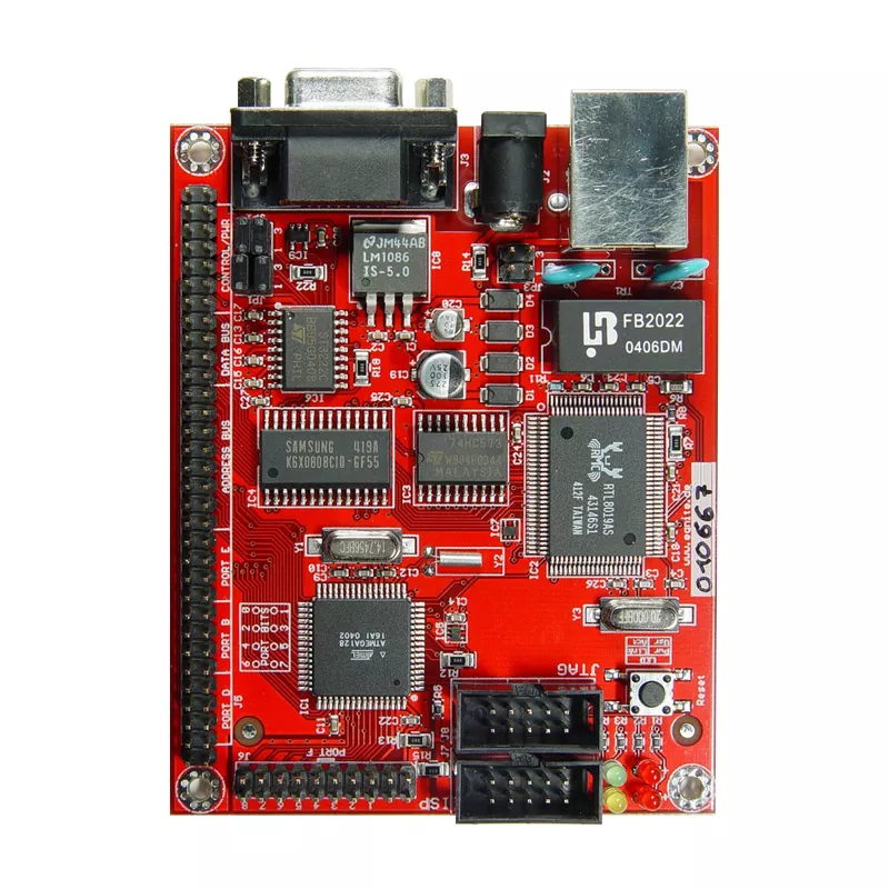
Are you looking for a way to optimize your electronic designs and improve the functionality of your products? Look no further than PCB design and layout!
PCB design and layout is a critical part of the electronics design process, involving the creation of a custom circuit board that connects and controls the various electronic components in a product. By optimizing the design and layout of your PCB, you can improve the performance and reliability of your products, while reducing costs and time-to-market.
One of the greatest benefits of PCB design and layout is its flexibility. PCBs can be designed to accommodate a wide range of components, such as resistors, capacitors, transistors, and microcontrollers, allowing for highly customized and specialized designs. Additionally, PCBs can be designed to fit almost any shape or size, making them ideal for use in a variety of products and applications.
Another key advantage of PCB design and layout is its ability to improve the functionality and reliability of electronic products. By carefully designing the placement and routing of components on the PCB, engineers can reduce signal interference, minimize noise, and improve the overall performance of the product. Additionally, PCBs can be designed with redundant components and fail-safe mechanisms, reducing the risk of product failure and improving reliability.
At our company, we specialize in PCB design and layout services, using the latest software and techniques to create custom circuit boards that meet the specific needs of our customers. Our experienced team of engineers and technicians work closely with our clients to understand their requirements and goals, and we use our expertise to deliver high-quality, efficient, and reliable PCB designs.
If you are looking to optimize the performance and reliability of your electronic products, contact us today to learn more about our PCB design and layout services. Let us help you take your designs to the next level and achieve success in your industry!
Produk
- View as

Pengantar keahlian kami dalam desain PCB
Dalam lanskap teknologi yang berkembang pesat saat ini, desain cetak sirkuit sirkuit (PCB) memainkan peran penting dalam pengembangan elektronik dan sistem modern. Di perusahaan kami, kami bangga sebagai pemimpin dalam pengenalan keahlian kami dalam desain PCB, bidang yang melibatkan tata letak strategis dan perakitan komponen elektronik pada permukaan datar untuk memastikan kinerja dan fungsionalitas yang optimal.
Baca selengkapnyamengirimkan permintaan
Desain dan tata letak PCB IoT
You are welcomed to come to our factory to buy the latest selling, low price, and high-quality IOT PCB design and layout, Hitech looks forward to cooperating with you.
Baca selengkapnyamengirimkan permintaan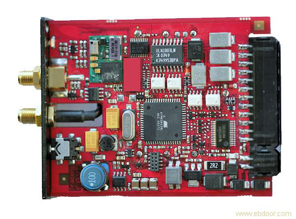
Desain PCBA Tracker Bluetooth
One of Chinese manufacturer of Bluetooth Tracker PCBA Design, offering excellent quality at a competitive price, is Hitech. Feel free to get in touch.
Baca selengkapnyamengirimkan permintaan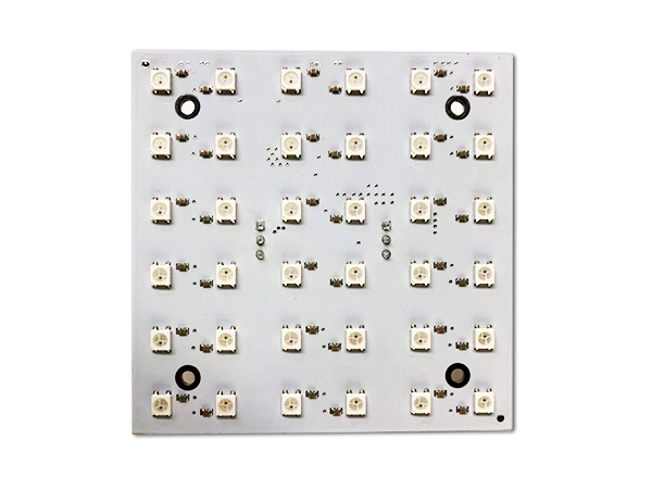
Desain dan manufaktur PCB IoT
Temukan banyak pilihan desain dan manufaktur IoT PCB dari China di Hitech. Berikan layanan purna jual profesional dan harga yang tepat, berharap untuk kerja sama.
Baca selengkapnyamengirimkan permintaan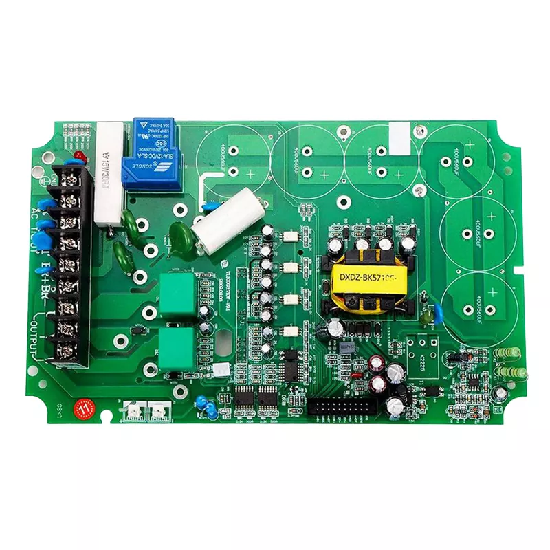
Layanan OEM ODM PCBA
Hitech adalah produsen dan pemasok layanan OEM ODM PCBA di Cina. Kami adalah penyedia layanan OEM/ODM PCBA terkemuka, menawarkan berbagai solusi untuk memenuhi kebutuhan unik Anda. Tim ahli kami berdedikasi untuk memberikan hasil yang luar biasa, bekerja sama dengan Anda untuk memastikan bahwa proyek Anda selesai dengan spesifikasi yang tepat. Fasilitas kami dilengkapi dengan teknologi dan peralatan canggih, memungkinkan kami untuk memberikan kualitas tinggi Layanan perakitan PCB yang efisien dan hemat biaya. Apakah Anda memerlukan prototipe sederhana atau perangkat elektronik yang rumit, kami memiliki pengalaman dan keahlian untuk memberikan hasil yang luar biasa.
Baca selengkapnyamengirimkan permintaan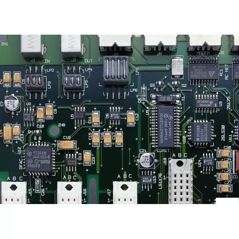
Prototipe PCBA
Hitech adalah produsen dan pemasok Prototipe PCBA profesional di China.Prototipe PCBA adalah langkah penting dalam proses desain elektronik. Ini melibatkan pembuatan sirkuit elektronik fungsional menggunakan PCB prototipe dan merakit komponen ke PCB untuk menguji dan memvalidasi desain. Proses prototipe PCBA sangat penting untuk memastikan kesuksesan produk elektronik Anda, dan dalam artikel ini, kami akan mengeksplorasi pentingnya prototipe PCBA dan faktor-faktor yang perlu dipertimbangkan saat membuat prototipe PCBA.
Baca selengkapnyamengirimkan permintaan
Hitech adalah produsen dan pemasok profesional Desain dan tata letak PCB di Cina. Kualitas tinggi kami Desain dan tata letak PCB tidak hanya dibuat di Cina dan kami memiliki produk yang disesuaikan. Selamat datang di pabrik kami untuk membeli produk.